Thursday, April 14, 2016

DAY 14: 1st order RC and RL Circiuts/ Passive RC and RL Circuit Natural Response

Part 1: 1st order RC and RL circuit
 Today, we discussed about the circuit RC or RL. We found the formula for current, voltage across the capacitor, and the inductor in each circuit.

First, we reviewed the inductance equivalent. Inductors in series and parallel circuit act as the resistors in series or parallel. 


Then, we analyzed a RC circuit free source, and measured the current across the capacitor. The voltage stored in the capacitor, we began to decrease by the time as v(t)=Vo*e^(-t/T), T=RC.

Mathematically, the voltage totally disappeared when the time is infinite. However, in terms of engineering, 1% voltage left is enough to consider that almost the voltage is gone. For the v(t)/Vo=1%, we have the time equal to 5*T, T=RC.Thus, when time equal 5T, we consider that the voltage is disappeared. 

the formula for the power of the circuit. 

In the ranges, R=[Rmin, Rmax], C=[Cmin, Cmax], the time constant min = Rmin*Cmin, the time constant max=Rmax*Cmax.

Part 2:  Passive RC and RL Circuit Natural Response Lab.

Purpose: The lab aims to help students verify their theory about the RC and RL circuit with the experiments. We will change the voltage by using the square voltage supply and disconnecting a DC. The will we compare the theoretical and experimental value of the time constant. T=RC or T=L/R.

Pre-lab:
We calculated the Theverin resistance of the circuit by replacing the voltage sources by short circuit or the current voltage by the open circuit. Then, R1//R2, We choose R1=1kOhm R2=2.2kOhm => Req= 0.6875kOhm. The time constant T=Re*C= 15ms

Then we set up the RC circuit according to the instruction. Use channel 1 to measure the voltage across the capacitor, and use the oscilloscope to get the voltage signal. 

First one we experiment by disconnecting the DC. We get the signal as the picture. The voltage across the capacitor almost disappeared in 100ms, and we know it by the previous analysis the time for almost this appearing about t=5T. So the T= 100ms/5=20ms. The theoretical is 15ms, so the percent difference is 33.33%.

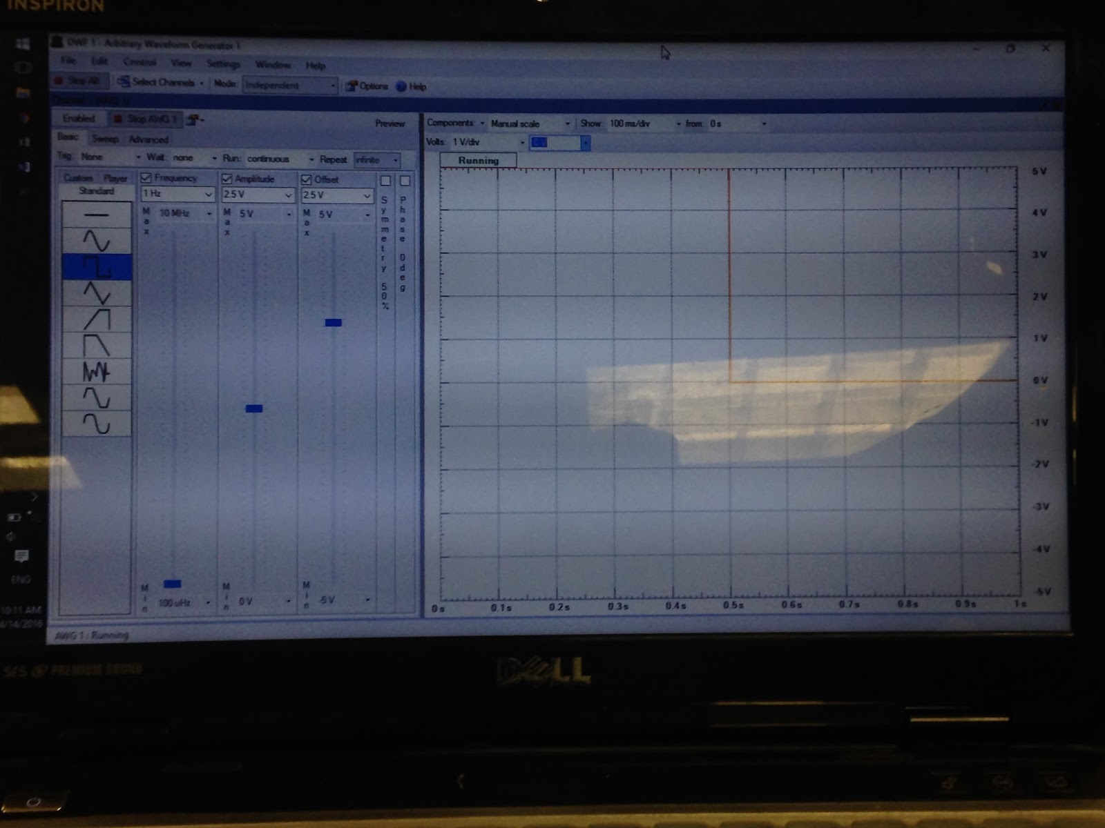
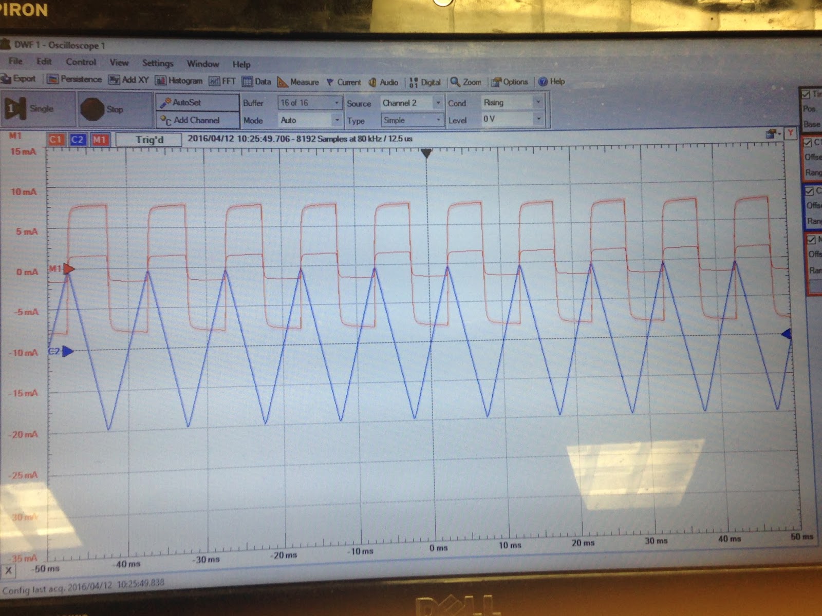
Then we created the square power supply by the waveform generator. 

The time constant for this experiment with a square power supply is 90ms/5= 18ms, so the percent difference is 20%.
The RL circuit:
The set-up is almost like the RC, only the difference is that we replaced the capacitor with a inductor. The time constant is T=L/R= 1mH/0.687kOhm=1.45us.

We replaced the capacitor with a inductor


The time constant for DC disconnection is T= 10us/5=2us. So this is off from the theoretical value. the percent difference is 40% 

For the square power supply, the time constant is 5us/5=1us, which is close to theoretical value. the percent difference is 31%. 
The difference is expected because the theoretical values are for a ideal capacitor and inductor. Because the real capacitor and inductor do not trapped the energy ideally, so we see there is the difference in the time constant. Moreover, as the theoretical the current in a inductor, or the voltage of the capacity totally disappear when the time is infinite. We assumed that that the appropriate time so that the current and the voltage are almost gone is 5T. There are two factors that affect our measurement.

Conclusion:
We discussed and analyzee the RC and RL free source. We also did some problem to gain the fundamental ideal how these elements work and deal with the resistors on the circuit. For the lab, we spent time working around to get the desired signal on the oscilloscope. We verified the natural response of the capacitor in RC circuit and the inductor in RL circuit. Due to the non-ideal capacitor and inductor as well as our assumption, our experimental values are likely different from the theoretical values. Despite that we still get the desired signals which express the natural response of the capacitor resisting to the change of voltage, and inductor resisting to the change of current. In the charging phrase or the very beginning moment, we will consider the inductor as the short circuit and the capacitor as the open circuit. 


DAY 13: Capacitors and Inductors/ Capacitor Voltage-current Relations Lab

Part 1: Capacitors and Inductors
We discussed about the capacitor and inductor. The professor introduced the properties of the capacitor and inuctors including current, voltage, power, and energy. 

The capacitor can storage the energy and release it to the circuit. The capacitor resists to the simultaneous change in voltage.  


The current of the voltage is i=C*dv/dt. So v=1/C*integral(i.dt). From the graph i vs. t, we can deduce the v vs. t


We did a practice problem on a circuit including two capacitors. We found the voltage and the energy in each capacitor.


Part 2: Capacitor Voltage-current Relations Lab

Purpose:
We will measure the relationship between the voltage difference across a capacitor and the current pass through it. We will apply several types of time-varying signals to a series combination of a resistor and a capacitor. 
Pre-lab:
We deduced the graph of i vs. t from the graph v vs. t of a capacitor. i=C.dv/dt. The resistor and the capacitor are in series, so the current through the capacitor is the same as the current through he resistor. ic(t)=Vr(t)/R.


The set-up for this experiment include a capacitor and a resistor in series. 

The sketches of the capacitor voltage and current for both sinusoidal and triangular input

The capacitor voltage and current waveform and the measured amplitude of the waveform for a 1kHz sinusoidal input. We observed the phase shift of voltage across a capacitor. The voltage across the capacitor lags the voltage across the resistor pi/2. phil(Vc)=phil(Vr)-pi/2.

The capacitor voltage and current waveform and the measured amplitude of the waveform for a 2kHz sinusoidal input.
The capacitor voltage and current waveform and the measured amplitude of the waveform for a 100Hz triangular input.


Here the picture of a capacitor after explosion. The professor did a experiment on a polarized capacitor. If we connect a polarized capacitor improperly, it will explode.

We deduced the inductor from the capacitor properties. And The professor gave the quick and brief summary of the capacitor and inductor on the table. 
In conclusion:
We examined the properties of the capacitor and inductor. We also did a experiment to observe the current and the voltage across a capacitor in a RC circuit. We found that the voltage across the capacitor lags the voltage across the resistor pi/2. phil(Vc)=phil(Vr)-pi/2. 

Friday, April 8, 2016

DAY 12: Cascaded Op Amps/ Temperature Measurement System Design

Part 1: Cascaded Op Amp

Today we discuss about cascaded op amp circuit, which means we make a circuit with more than one op amp. 


A cascaded op amp circuit including the inverting summing op amp with two other inverting op amp. 


A cascaded circuit includes two non-inverting op amps. We apply the formula of the non-inverting op amp for each op amp. v(out) = (Rf+Rs)/Rs * v(in) (deduce from nodal analysis or voltage divider). To find the current i(10k)=[v(out2) - v(out1)] / 10k.


Digital - Analog Circuit. 
The digital-to-analog converter DAC transforms digital signal into analog form. The bits are weights according to the magnitude of their place value, be descending value of Rf/Rn so that each lesser bit has half the weight of the next higher.


Instrumentation amplifier. 
It is used for precision measurement and process control. Typical application of IA includes isolation amplifier, thermocouple amplifiers, and data acquisition systems. Function is an extension of the difference amplifier in that it amplifies the difference between its input signals.
the formula of the instrumentation amplifier. It show the different input voltages is amplified by the constant gain. If all resistances are equal except R4, called Rg, then the gain A equal 1 + 2R/Rg.

Part 2: Temperature Measurement System Design

Purpose:
We apply the theory of the Wheatstone Bride Circuit and the Difference amplifier to operate this experiment and set-up the temperature measurement System Design. The requirements are,
1. The out voltage from the system is balance 0 +/- 20mV at room temperature,
2. Output voltage is positive for temperature above the room temperature,
3. he output voltage increase by a minimum of 2V over a temperature range of 25 degree Celsius - 37 degree Celsius.


Pre-lab: 
1. Wheatstone Bridge Circuits: most often used to convert variations in resistance to variations in voltage. This is applied for some common sensors providing a resistance variation in response to some external influence, some of those we have discussed: thermistors(temperature), strain gages(deformation), photoconductive transducers(light intensity).

From voltage division analysis of va and vb, we have: v(ab)=va-vb= - [delta(R)/(4R)]*Vs-> v(ba)=[delta(R)/(4R)]*Vs


2. Difference amplifier: we apply the condition when R1/R2=R3/R4, then vo = R2/R1 * (vb-va) =R2/R1 *v(ba).

3. The thermistor changes as the temperature changes, Ro+delta(R), with Ro is the initial temperature at room temperature.

So, the expected process is that the change in temperature of thermistor lead to the change in resistance, then change of v(ab), the change in vo which we want to increase a minimum of 2 V

Set-up and resutls:

We set up the experiment as the video below, the videos show that the requirement results are satisfied:


Conclusion:
To analyze a cascaded op amp circuit, we either use the nodal technique to analyze this circuit or use the formulas for each kind of op amp set-up including 
1. inverting op amp: vo=(-Rf/Rs)*vi 
2. non-inverting op amp: vo= (1+Rf/Rs)*vi
3. summing amplifier: vo = Rf( v1/R1 + v2/R2 + v3/R3 +....)
4. difference amplifier: vo= Rf/Rs *[vi(noninverting) - vi(inverting)], if R1/R2 = R3/R4. 
We did some practical problems of a cascaded circuit. We also discuss about Wheatstone and how to balance the bridge circuit. We did the lab on the temperature Measurement System Design, which combine the theory of the Wheatston Bridge Circuit and the Different amplifier. We get the expected result that qualify the requirements: the out voltage from the system is balance 0 +/- 20mV at room temperature, output voltage is positive for temperature above the room temperature, and the output voltage increase by a minimum of 2V over a temperature range of 25 degree Celsius - 37 degree Celsius.

Tuesday, April 5, 2016

DAY 11: Op Amp 2/ Summing Amplifier Lab

Part 1: Op amp (cont.)
Today we continue to study some different op amp circuit. 

Sinusoidal graph transformation. From the original f(t) voltage source, assuming that it goes through the op amp to shift its values above. There are two ways of shifting the graph: plus then add, or add then plus.Both ways have the same result. Two characteristics of the op amp that help to build this kind of circuit are the gain between the output and the input voltages, the limitation of the power supply voltage on the output voltage. The first process to create the desired graph is let the Vin go through the op amp with gain 25, then place the 25 DC voltage in series with the output voltage. The second process is we use summing amplifier to create the voltage Vout = A(V(in1) +V(in2)).

This is inverting op amp. Assuming the op amp is ideal with vp=vn and ip=in=0. From the circuit we have vp=0, then vn=0. We use the nodal analysis at vn, [v(in)-0]/Rs +[v(out)-0]/Rf = 0=> v(out)=(-Rf/Rs) *v(in). This formula also express the inverting characteristic of op amp with negative gain. From the formula and the limitation of the power supply on the output voltage, we deduce the output voltage as the picture describes: being inverted, and above the horizontal axis.  


This is a different amplifier. 

Non-inverting op amp. We derive the relationship between the V(out) and V(in) as
V(out)=[-(Rs+Rf)/Rf] * V(in) = -(1+Rs/Rf)*V(in). Rf<<Rs => Vout =Vin. Vout is always equal or greater than V(in) for the non-inverting op amp.

The unity gain buffer amplifier is to create the independence in the circuit, The output voltage equals to the input voltage but has a larger current because of the power supply. 


Part 2: Summing Amplifier Lab
Purpose: The lab aims to give students the ideal how a summing amplifier works, and verify the theory of the summing amplifier
A summing amplifier. Like the name of the op amp setup, the output voltage is the summing of the input voltage with appropriate constant. We notice the two create the summing amplifier the input voltages have to go into the same input terminal, in this case is the inverting input. Using the nodal analysis at inverting input, we retrieve the relationship between the output voltage and three input voltages, or more.

We do the pre-lab for a summing amplifier. The requirement is to create the output voltages were not saturated at all. From the general summing amplifier formula, we should choose R1=R2 to let the math more easily. Because we do not want to see the saturation, we choose R3 less than R1=R2. With the nodal analysis at inverting input and ideal op amp assumption, we deduce the formula, 
V(out)=[-R3/R1]*(Va+Vb)
Vb is always 1V; we adjust Va to get the output voltage. The record is in the table. We get acceptable data, which meets our expectation and deduction. 


Our experimental set-up
 After the lab, the professor talk little bit about organized breadboard set-up. We should avoid cross wire or component, and advice to use different color wires such as red for positive, black for ground, yellow, blue, green for signal, and use different length wires. An organized set-up will help us follow the circuit and check any existing errors easily.


In the end, we discuss about the different op amp. We have a talk about the above circuit type (inverting, noninverting, summing, different). By nodal analysis t vn and vp or the voltage divider at vn and vp, we deduce that v(out)=0.3 v2. This deduction is the same as we consider that this circuit is the different op amp with va=0, vb=+/-5V. By applying the different op amp formula for the condition R1/R2 =R3/R4, we get the same result as the nodal analysis as 
V(out)=R2/R1(Vp-Vn)=> Gain A = 33/100 = 0.33

Conclusion:
Today, we understand more about the op amp and discuss some popular om amps: the noninverting, summing, unity buffer amplifier, difference amplifier. For each kind of op amp, we use the nodal analysis to express the relationship between the output voltage and the input voltage. Also, we did 
the lab of summing amplifier, We practice to sense intuitively the resistors' values for no saturation in the op amp summing amplifier. We get the measured values matching the our expectation.

Monday, April 4, 2016

Day 10: Op Amp/ Op Amp Lab

Part 1: Op Amp 

Today, we study about op amp and its structure and properties. 


The terminals of primary interest are: inverting input, noninverting input, output, positive power supply, negative power supply. 
The voltage transfer characteristic describes how the output voltage varies. There are 3 distinct regions of operation. Based on the values of the difference of the input voltages, the output voltage is a linear function of the input voltages or saturates. A is the multiplying constant or gain. 


Then the professor asked us what are the open loop and the closed loop. In terms of electric circuits, the closed loop is when a signal is fed back from the output terminal to the inverting input terminal(-), also called negative feedback. While the open loop is when the circuit has no feedback. 


The professor introduce about a op amp practice. We use the realistic op amp with a large input resistor, a large gain, and a small out resistor. By applying the nodal technique at the inverting input voltage (Vn), and the output voltage (Vo), we gain two equation and solve for Vn, Vo. We calculate the gain by A=Vout/Vin

The ideal op amp. We retrieve two conditions for the ideal op amp. The first one is the constraint on input voltage of the op amp: Vn = Vp. Consequently, the gain A is infinite. The second condition is the current constraint ip = in = 0. Analysis of the op amp integrated circuit reveals that the equivalent resistance seen by the input terminals of the op amp is very large, typically 1M Ohm or more. 

Part 2: The Inverting Voltage Amplifier

Purpose: The lab aims to put the theory of the op amp into the realistic experiment. Specifically, we analyze the inverting voltage amplifier with a closed loop. We expect to retrieve the graph with three distinct regions of an op amp. 

We do the pre-lab to find the value of R2 so that we designed an amplifier which provides a gain of 2 and an input resistance R1 =2k Ohm. We end up with R2 = 4k Ohm. From the condition of an ideal op amp and the nodal analysis at the inverting input, we get vo=-(R2/R1)*vi. 
The guidance for setting up an op amp OP27 on the breadboard.


We set up the experiment, then adjust the input voltage and record the output voltage values. 


The measured output voltage table and the graph Vin vs. Vout. We observe that the graph has 3 distinct region as a op amp's property: positively saturated region, linear region, negatively saturated region. Besides, the negative and positive saturation are not equal to the value of the power supply because of the imperfection of a an op amp.

The professor's explanation why the saturation is not equal to the power supply value. This is called rail to rail performance, op amp effective measurement.


Conclusion:
We learned about a new concept/component of electric circuits: op amp. We discussed how to distinguish  between the open loop and the closed loop by the negative feedback of the inverting input. We also discussed on three conditions of the ideal op amp: infinite input resistance, infinite gain, zero input current. In the experiment, we observe the op amp property with the graph v(in) vs. v(out), and the rail to rail performance.